https://amtek.wordpress.com/2010/10/24/eagle-tutorial/
Eagle Schematic and PCB tutorial
Posted: October 24, 2010 in Tutorials
Tags: eagle, pcb, schematic
This tutorial will show you how to make a pcb right from creating the schematic and board layout to actually etching the pcb.
Since the tutorial will get a little big, Im gonna split it into two
parts. The first will deal with creating the schematic and the board
layout and the second will be about etching the pcb.
Anyone who has done a reasonably sized project on electronics knows
how tedious it is to solder each and every component and its connection
on a GPCB(General Purpose circuit board), not to mention the amount of
short circuits you’ll have before you get it working. If you don’t want
your circuit to fail in the middle of demonstration or a competition
then its best to do it on a pcb. This tutorial is aimed specifically at
people who just want to build and test their prototype quickly and don’t
want to spend money getting it etched from a professional(which usually
costs around
Rs.800 for an average sized board). So let’s get started…
To design the schematic and the pcb layout, we’ll be using EAGLE
which is a tool created for just that. It has a large number of parts
and if you don’t find one that you need, you can create one yourself
very easily. You can download the light version
here,
it has all the features that the professional version does. The only
limitation being that the board size can’t exceed 10cmx8cm. If you want
to make bigger boards then you can purchase the professional version
(I’m sure you can figure out how to get it without paying but just
remember that its illegal if you want to use it professionally).
I just use EAGLE because it’s the first tool I used to create PCB’s
and I’ve been using it ever since. There are other PCB editors like
DipTrace, EasyPCB etc which provide better UI and autorouting options
than eagle. Once you know how to use EAGLE, you can use the other
editors with ease.
To get you acquainted with the basics of EAGLE we’ll be designing a simple LED flasher using the 555 IC.
After downloading and installing EAGLE, open it and create a new project and give it a name(It’ll be a folder icon under eagle).

Then create a new schematic by going to File>New> Schematic.
EAGLE doesn’t ask you a name like most other apps so its better if you
save it with a unique name or else you’ll end up with a bunch of files
called “untitled”. You’ll get a screen like this
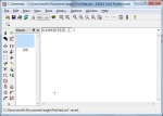
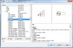
Click on the Add button on the left toolbar, this dialog will let you
access all the parts available in eagle but the search function isn’t
that great, you can however, search using a wildcard character if you
don’t know the exact part number. For example, search for “*555” and
select ne555 from the list .


Place the device anywhere you want using the left mouse button.

Next we’ll add resistors which can be found in the same ADD dialog,
but EAGLE has a lot of packages for resistors and capacitors which can
be a bit confusing for a beginner. Search for “resistor” in the search
box
and you’ll get a bunch of results, choose resistor>R-US_ and select the 10mm package.

Now place four resistors as shown.

Now we’ll place capacitors. Click on ADD again and search for
“capacitor” and select rcl>CPOL-US and select the 5mm package and
place it on the layout. Add another capacitor but this time an 8mm
package. It doesn’t matter in which library you find the package as long
its of the correct size.

After you’ve placed them, it should look something like this

(C1 is the 5mm package and C2 is the 8mm package)
Now we’ll place two LED’s by searching for “LED” and selecting
led>LED and then the 5mm package. If you want to rotate any part to
fit the schematic, you can do so by selecting the component and clicking
the right mouse button.

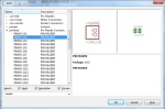
Now we’ll place a potentiometer, again click on ADD, search for
“potentiometer” and select pot>TRIM_US and S64W package. Im choosing
this package because this is the actual pot that ill be using on the
PCB, if you have a different type of pot then choose the right one.


If you want to move any component around, select the “move” button
from the left toolbar and select on the component you want to move and
move it around. If it’s a big component then just pressing inside the
empty space inside it wont move it, you have to select it using the +
mark inside the component. I found this out after a lot of cursing.
Now we’ll place a two pin header for connecting the power supply.

Now we’ll name all the components so they’re easier to recognize.
Select the Info button

and click on R4 and type in “1.5K” in the value box.
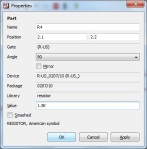
Do the same for R1(470Ω),R2(470Ω) , R3 (1.5K) and R5(220K).
Now assign the values for the capacitors. C1 is 10uF and c2 is 100uF.
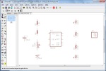
Now we’ll begin connecting all the components. To easily connect
wires you can choose to see the pins by going to view>Display/Hide
Layers and selecting Pins. Now Select the wire tool and click on one of
the pins and move your mouse to the other pin which you want to connect
and click on it. If you want to stop the connection on a pin then you
have to double click on that pin or you can press escape after you’ve
connected it. Make the connections as shown.

If you’re not sure whether the connection has taken place to a
certain component then select the move button and move the component
around, if the wire also moves around with it, it means its connected.
If not, select the delete tool and remove the wire and re-connect.
After everything is done, click on the info button and then click on any
wire which is connected to VCC and change its name to “VCC”, it would
be something like N$10. Do the same for the ground wire and name it
“GND”. This is needed later when designing the PCB layout.
That’s it for the schematic. If you want you can add a frame containing
the details in case you have to submit it somewhere by going to ADD and
searching for “frame” and selecting whichever size you want.
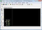
Now we’ll move onto actually designing the PCB. Click on the Board button

present on the top toolbar and select yes when it asks if you want to
create a new board. You’ll get a new window which has a black
background containg all the parts jumbled together on one side. There’s a
white border towards the right, this is the actual workable area of the
PCB. You can resize the size of the PCB using these white lines.
Now its obvious that you want your PCB to be as small as possible but
you wont know how small you can make it until you try placing the
components. In any circuit, start with the main component in the center
and put the others around it. You can then see how they actually connect
to each other and move them around if necessary.
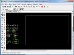
Start by reducing the workable area to a size slightly bigger than you
want. To do this, select the move tool, click on the right most line and
bring it towards the left. Do the same for the top line and bring it
down to reduce the size, you should get something like this-
Now select the 555 IC and move it towards the center.

Ok so I just realized I’ve made a mistake in the schematic, instead
of connecting one of the wires to the middle of the pot, I’ve connected
it to the other end. But its not a big deal, you can just go back to the
schematic and correct it. If you do so, you’ll see that it
automatically gets updated in the board layout too.
The wrong connection is shown as a red cross mark.
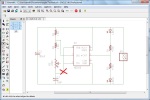
Use the delete button to delete the wrong connection and re-connect it using the wire tool.
The corrected version –

Now move all the other parts around until they look something like this. Again, to rotate a part use the right click.
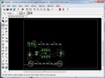
I’ve moved all the parts towards the left- bottom corner. To do this,
click on the selection box tool and create an area around all the
parts, then select the move button and right click on any part and click
move group and move it to the corner.
To re-route the air wires to their closest points you can go to Tools and select ratsnest.
We can now reduce the PCB area even more since we have a lot of empty space.
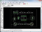
Before we begin routing wires we have to set the properties of the
routing like minimum width of the wire, spacing between the wires etc.
These are called “Design rules” and the default rules in EAGLE are not
exactly hobbyist friendly so it has to be tweaked a little. I’ve
uploaded a file containing the Design rules that I use so you can use it
directly, or you can set the values yourself.
Download the Desing Rules File here
If you want to use the file I’ve uploaded, go to Edit> Design rules, click on Load and select the file and click OK.
If you want to change it manually, these are the settings

This sets the minimum distance between two routings.
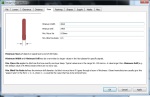
This is for the minimum width of the wire.
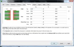
I haven’t changed anything in this but this is to set the size of the pads and vias.
After setting the rules we can now start routing. EAGLE has a decent autorouter which you can use for small circuits.
Go to Tools and select autorouter, this dialog will let you access the
routing settings like number of layers, cost of each layer etc. Select
NA for top layer and ‘–‘ for bottom layer since we’re doing only a
single sided board.

After you click OK, you’ll see a bunch of blue lines, these are the
actual copper traces. If you use this layout to etch it’ll work but it’s
always a good idea to add a power plane to the circuit. A power plane
is a large area on the layout which is connected to either VCC or
ground. There are many reasons to add a power plane, it’ll reduce the
amount of etchant required, it’ll help the toner stick better and it’ll
help carry large currents in case your circuit needs it. You can do
this by selecting the polygon tool from the left toolbar and drawing a
box around the layout like this-

Click on the info button and then on the polygon and type in the
isolate value as 1.2 and name as “VCC”. The isolate value defines the
minimum clearance between the plane and any other signal. The name you
give connects the plane to that signal. If you cant rename it, go to
edit> name, click on the polygon and rename it.
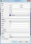
Now go to tools and press ratsnest, you should get something like this-

If it gives an error saying wrong polygon or something like that then you have to do the following.
Zoom in on the point where you ended the polygon, mine was upper left corner
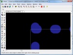
You can see there are multiple dots there, you have to delete one of them so that it looks like this.

Now try ratsnest again and it should work.
Now create one more polygon as before but this time only update the
isolate value and leave the name as whatever it is. You cannot add two
power planes in a single layer, so this polygon will just fill empty
spaces with copper without connecting it to anything. This will reduce
the amount of etchant required to etch the pcb.

Well that’s the final PCB layout which you can use to etch. I haven’t
covered all the concepts but I hope its enough to get you started.
There are a few things I’d like to mention,
1. There’s no option to undo the wires created by the autorouter. To
delete them, select all the wires using the selection box, select rip-up
and right click on any wire and press rip-up all.
2. Most of the time the routing wont be 100%, so you’ll have to use some
external wires, to do this you have to add vias where you want to
connect external wires and route them manually.
3. To hide/unhide any layers use the Display/hide layers dialog found in the View menu.
A tutorial on etching the PCB is coming soon.
This is my first tutorial so hope I didn’t mess it up. If you have any questions or comments, leave them below.