Sidetone Oscillator with 2N3904/3906
The second sidetone oscillator is build up completely discrete with two transistors and four passive components. The VT1 and VT2 arrangement corresponds to the thyristor substitute circuit, but with something special. Not the emitter of VT2 but the VT2 collector is connected to Gnd potential.
If one runs VT2 as usual with the emitter connected to ground, VT1 and VT2 together have a very high current gain. This high gain causes that the low current flow through R1 (C1 is discharged via VT1) is sufficient high that both transistors remain in the on state. Hence periodically charging and discharging the capacitor is impossible, because the hold on current will never be fallen below. A measure against this effect could be a low impedance voltage divider R2/R3 in order to take over a partial current (Ic_VT2) or a gain reduction. The later is achieved very easy with the reverse operation of VT2. The hold on current is fallen and thus VT1 and VT2 return to the off state after discharging C1.
Now the circuit operates as planed. C1 will be charged by a low current via R1 up to the voltage rate Uc = Ux + 0,7 V. A small basis current flows into VT1 as soon as Uc exceeds the limit value Ux + 0,7 V. VT2 conducts too by the now starting collector current. On the basis of the positive feedback both transistors are conducting quickly and VT2 discharges the capacitor immediately. The collector current defined by R1 is lower than the hold on current required for VT1 and VT2. Both transistors go back to the non-conducting state and the game starts from the beginning.
Fig.1: Discrete designed oscillator
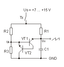
The advantage of the circuit is the excellent frequency stability a supply voltage changes. If the supply voltage decreases the charging time of C1 rises and thus the frequency. Because the limit value Ux decreases at the same time the frequency rises thereupon. The achievable compensation with the specified components within the voltage range Us = +7 ... +15 V is nearly perfect. The difference to the 650 Hz nominal frequency is only +/- 5 Hz. At 2 V supply voltage the saw tooth signal amplitude at the output is 2,5 Vss. The Tx control signal can not only switch off and on the the complete circuit but it can also supply it due to the low current consumption of less than 0,5 mA. The Us terminal is not necessary then.
| Parts | Value |
|---|---|
| R1 | 120 kOhm |
| R2 | 22 kOhm |
| R3 | 6,8 kOhm |
| C1 | 0,047 uF |
| VT1 | 2N3906 |
| VT2 | 2N3904 |
No hay comentarios:
Publicar un comentario